Welcome to DU!
The truly grassroots left-of-center political community where regular people, not algorithms, drive the discussions and set the standards.
Join the community:
Create a free account
Support DU (and get rid of ads!):
Become a Star Member
Latest Breaking News
General Discussion
The DU Lounge
All Forums
Issue Forums
Culture Forums
Alliance Forums
Region Forums
Support Forums
Help & Search
Environment & Energy
Related: About this forumPerovskite edges can be tuned for optoelectronic performance
(Please note: Materials from Los Alamos National Laboratory—Copyright concerns are nil.)
http://www.lanl.gov/discover/news-release-archive/2017/March/03.09-perovskite-edges.php
[font face=Serif][font size=5]Perovskite edges can be tuned for optoelectronic performance[/font]
[font size=4]Scientists are creating innovative 2D layered hybrid perovskites that allow greater freedom in designing and fabricating efficient optoelectronic devices.[/font]
March 9, 2017
Scientists at Los Alamos National Laboratory and their research partners are creating innovative 2D layered hybrid perovskites that allow greater freedom in designing and fabricating efficient optoelectronic devices.Scientists at Los Alamos National Laboratory and their research partners are creating innovative 2D layered hybrid perovskites that allow greater freedom in designing and fabricating efficient optoelectronic devices.
[font size=4]Layered 2D material improves efficiency for solar cells and LEDs[/font]
[font size=3]LOS ALAMOS, N.M., March 9, 2017—In the eternal search for next generation high-efficiency solar cells and LEDs, scientists at Los Alamos National Laboratory and their partners are creating innovative 2D layered hybrid perovskites that allow greater freedom in designing and fabricating efficient optoelectronic devices. Industrial and consumer applications could include low cost solar cells, LEDs, laser diodes, detectors, and other nano-optoelectronic devices.
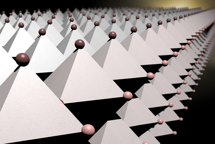
“Our material is a layered compound, meaning it is a stack of 2D layers of perovskites with nanometer thickness (like a stack of sheets), and the 2D perovskite layers are separated by thin organic layers,” said Jean-Christophe Blancon, lead author on a paper out today in the journal Science’s First Release distribution. “This work could overturn conventional wisdom on the limitations of device designs based on layered perovskites.”
The 2D, near-single-crystalline “Ruddlesden-Popper” thin films have an out-of-plane orientation so that uninhibited charge transport occurs through the perovskite layers in planar devices. At the edges of the perovskite layers, the new research discovered “layer-edge-states,” which are key to both high efficiency of solar cells (>12 percent) and high fluorescence efficiency (a few tens of percent) for LEDs. The spontaneous conversion of excitons (bound electron-hole pairs) to free carriers via these layer-edge states appears to be the key to improving the photovoltaic and light-emitting thin-film layered materials.
The team investigated both photophysical and optoelectronic properties of phase-pure homogenous 2D perovskites. They were able to show that thin films have an intrinsic mechanism for dissociation of the strongly bound electron-hole pairs (excitons) to long-lived free-carriers provided by lower energy states at the edges of the layered perovskites.
Moreover, once carriers are trapped in these edge states, they remain protected and do not lose their energy via non-radiative processes. They can contribute to photocurrent in a photovoltaic (PV) device or radiatively recombine efficiently for light-emission applications. “These materials are quantum hybrid materials, possessing physical properties of both organic semiconductors and inorganic semiconducting quantum wells. We are just beginning to understand the interplay of the organic and inorganic components in 2D perovskites and this result underpins how unique properties can arise from competing physical properties,” said Jared Crochet of the Physical Chemistry and Applied Spectroscopy group at Los Alamos.
“These results address a long-standing problem not just for the perovskite family, but relevant to a large group of materials where edges and surface states generally degrade the optoelectronic properties, which can now be chemically designed and engineered to achieve efficient flow of charge and energy leading to high-efficiency optoelectronic devices,” said Aditya Mohite, who leads the perovskite program in the Material Synthesis and Integrated devices group at Los Alamos.
“The 2D hybrid perovskites continue to surprise. When we first designed these materials we were hoping that high quality samples of them would exhibit novel optoelectronic properties,” said co-author Mercouri Kanatzidis of Northwestern University. “Well, they have done so and then some. They have exceeded our expectations and are proving to be truly amazing systems. We have only scratched the surface of what is there—sorry for the pun—in this 2D family and we anticipate continued excitement going forward.”
The paper: “Extremely efficient internal exciton dissociation through edge-states in layered 2D perovskites,” J.-C. Blancon, W. Nie, S. Tretiak, J. J. Crochet and A. D. Mohite of Los Alamos National Laboratory; H. Tsai and P. M. Ajayan of Rice University, Houston, Texas; C. C. Stoumpos, C. M. M. Soe, and M. G. Kanatzidis of Northwestern University, Evanston, Illinois; L. Pedesseau and J. Even of Fonctions Optiques pour les Technologies de l’Information (FOTON), INSA de Rennes, France; C. Katan and M. Kepenekian of Institut des Sciences Chimiques de Rennes (ISCR), Université de Rennes, France; K. Appavoo and M. Y. Sfeir of Brookhaven National Laboratory, Upton, New York.
…
…[/font][/font]
[font size=4]Scientists are creating innovative 2D layered hybrid perovskites that allow greater freedom in designing and fabricating efficient optoelectronic devices.[/font]
March 9, 2017
Scientists at Los Alamos National Laboratory and their research partners are creating innovative 2D layered hybrid perovskites that allow greater freedom in designing and fabricating efficient optoelectronic devices.Scientists at Los Alamos National Laboratory and their research partners are creating innovative 2D layered hybrid perovskites that allow greater freedom in designing and fabricating efficient optoelectronic devices.
[font size=4]Layered 2D material improves efficiency for solar cells and LEDs[/font]
[font size=3]LOS ALAMOS, N.M., March 9, 2017—In the eternal search for next generation high-efficiency solar cells and LEDs, scientists at Los Alamos National Laboratory and their partners are creating innovative 2D layered hybrid perovskites that allow greater freedom in designing and fabricating efficient optoelectronic devices. Industrial and consumer applications could include low cost solar cells, LEDs, laser diodes, detectors, and other nano-optoelectronic devices.
“Our material is a layered compound, meaning it is a stack of 2D layers of perovskites with nanometer thickness (like a stack of sheets), and the 2D perovskite layers are separated by thin organic layers,” said Jean-Christophe Blancon, lead author on a paper out today in the journal Science’s First Release distribution. “This work could overturn conventional wisdom on the limitations of device designs based on layered perovskites.”
The 2D, near-single-crystalline “Ruddlesden-Popper” thin films have an out-of-plane orientation so that uninhibited charge transport occurs through the perovskite layers in planar devices. At the edges of the perovskite layers, the new research discovered “layer-edge-states,” which are key to both high efficiency of solar cells (>12 percent) and high fluorescence efficiency (a few tens of percent) for LEDs. The spontaneous conversion of excitons (bound electron-hole pairs) to free carriers via these layer-edge states appears to be the key to improving the photovoltaic and light-emitting thin-film layered materials.
The team investigated both photophysical and optoelectronic properties of phase-pure homogenous 2D perovskites. They were able to show that thin films have an intrinsic mechanism for dissociation of the strongly bound electron-hole pairs (excitons) to long-lived free-carriers provided by lower energy states at the edges of the layered perovskites.
Moreover, once carriers are trapped in these edge states, they remain protected and do not lose their energy via non-radiative processes. They can contribute to photocurrent in a photovoltaic (PV) device or radiatively recombine efficiently for light-emission applications. “These materials are quantum hybrid materials, possessing physical properties of both organic semiconductors and inorganic semiconducting quantum wells. We are just beginning to understand the interplay of the organic and inorganic components in 2D perovskites and this result underpins how unique properties can arise from competing physical properties,” said Jared Crochet of the Physical Chemistry and Applied Spectroscopy group at Los Alamos.
“These results address a long-standing problem not just for the perovskite family, but relevant to a large group of materials where edges and surface states generally degrade the optoelectronic properties, which can now be chemically designed and engineered to achieve efficient flow of charge and energy leading to high-efficiency optoelectronic devices,” said Aditya Mohite, who leads the perovskite program in the Material Synthesis and Integrated devices group at Los Alamos.
“The 2D hybrid perovskites continue to surprise. When we first designed these materials we were hoping that high quality samples of them would exhibit novel optoelectronic properties,” said co-author Mercouri Kanatzidis of Northwestern University. “Well, they have done so and then some. They have exceeded our expectations and are proving to be truly amazing systems. We have only scratched the surface of what is there—sorry for the pun—in this 2D family and we anticipate continued excitement going forward.”
The paper: “Extremely efficient internal exciton dissociation through edge-states in layered 2D perovskites,” J.-C. Blancon, W. Nie, S. Tretiak, J. J. Crochet and A. D. Mohite of Los Alamos National Laboratory; H. Tsai and P. M. Ajayan of Rice University, Houston, Texas; C. C. Stoumpos, C. M. M. Soe, and M. G. Kanatzidis of Northwestern University, Evanston, Illinois; L. Pedesseau and J. Even of Fonctions Optiques pour les Technologies de l’Information (FOTON), INSA de Rennes, France; C. Katan and M. Kepenekian of Institut des Sciences Chimiques de Rennes (ISCR), Université de Rennes, France; K. Appavoo and M. Y. Sfeir of Brookhaven National Laboratory, Upton, New York.
…
…[/font][/font]
InfoView thread info, including edit history
TrashPut this thread in your Trash Can (My DU » Trash Can)
BookmarkAdd this thread to your Bookmarks (My DU » Bookmarks)
0 replies, 893 views
ShareGet links to this post and/or share on social media
AlertAlert this post for a rule violation
PowersThere are no powers you can use on this post
EditCannot edit other people's posts
ReplyReply to this post
EditCannot edit other people's posts
Rec (3)
ReplyReply to this post